ADC INTERFACING WITH 8051
ADC is required to convert the output of the sensor, which is analogue in nature to a digital form.
Synopsis

In many applications ADC is required to convert the output of the sensor, which is analogue in nature to a digital form. The data in digital format can then be utilized for further processing by the digital processors. Typical applications include sound processing, temperature processing etc. ADC0804 is one of the most commonly used analog to digital converter IC.

Description

ADC0804 which is an 8-bit resolution ADC has only one input channel connected to variable resistance (preset) to give the analog input. In place of preset, analog input from a sensor can also be used. The output pins of the ADC are connected to GPIO port of the microcontroller.

ADC0804 is a single channel analog to digital convertor i.e., it can take only one analog signal. An ADC has n bit resolution (binary form) where n can be 8,10,12,16 or even 24 bits. ADC 0804 has 8 bit resolution. The higher resolution ADC gives smaller step size. Step size is smallest change that can be measured by an ADC. For an ADC with resolution of 8 bits, the step size is 19.53mV (5V/255).

The time taken by the ADC to convert analog data into digital form is dependent on the frequency of clock source. ADC0804 can be given clock from external source. It also has an internal clock. However the conversion time cannot be more than110us. To use the internal clock a capacitor and resistor is connected to pin 19 and 4.

The frequency is given by the relation f= 1/ (1.1RC). The circuit uses a resistance of 10k and a capacitor of 150pF to generate clock for ADC0804. Vin, which is the input pin, is connected to a preset to provide analog input.

Pin Description


1. CS, Chip Select: This is an active low pin and used to activate the ADC0804.

2. RD, Read: This is an input pin and active low. After converting the analog data, the ADC stores the result in an internal register. This pin is used to get the data out of the ADC 0804 chip. When CS=0 & high to low pulse is given to this pin, the digital output is shown on the pins D0-D7.

3. WR, Write: This is an input pin and active low. This is used to instruct the ADC to start the conversion process. If CS=0 and WR makes a low to high transition, the ADC starts the conversion process.

4. CLK IN, Clock IN: This is an input pin connected to an external clock source.

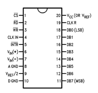
5. INTR, Interrupt: This is an active low output pin. This pin goes low when the conversion is over.

6. Vin+: Analog Input.

7. Vin- : Analog Input. Connected to ground.

8. AGND: Analog Ground.

9. Vref/2: This pin is used to set the reference voltage. If this is not connected the default reference voltage is 5V. In some application it is required to reduce the step size. This can be done by using this pin.

10. DGND: Digital Ground.

11. 11-18. Output Data Bits (D7-D0).

12. 19 CLKR: Clock Reset.

13. 20 Vcc: Positive Supply

Proteus design for ADC interfacing with 8051


Orcad design for ADC interfacing with 8051


ADC interfacing with 8051

/*  Name     : main.c
 *  Purpose  : Source code for ADC0804 Interfacing with AT89C52.
 *  Author   : Gemicates
 *  Date     : 2014-02-15
 *  Website  : www.gemicates.org
 *  Revision : None
 */
 

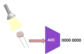
 //Program to check the working of ADC0804 using LED's on its output port.
#include <REGX52.H>

#define input P2  				// Input port to read the values of ADC
#define output P0  				// Output port, connected to LED's.

sbit wr= P1^1;  				// Write pin. It is used to start the conversion. 
sbit rd= P1^0;  				// Read pin. It is used to extract the data from internal register to the output pins of ADC.
sbit intr= P1^2;  				// Interrupt pin. This is used to indicate the end of conversion. It goes low when conversion is complete.

void delay(unsigned int msec )                  // The delay function provides delay in msec.
{
	int i,j ;
	for(i=0;i<msec;i++)
  for(j=0;j<1275; j++);
}

void adc()  					// Function to read the values from ADC and display on the LED's.
{
	rd=1;     
	wr=0;     
	delay(1);
	wr=1;
	while(intr==1);
	rd=0;
	output=input;
	delay(1);
	intr=1;
}

void main()
{
  input=0xff;  					// Declare port 0 as input port.       
	while(1)
	{
   adc();
  }
}
DATA SHEET FOR ATMEL_89C52

Error message here!

Show Error message here!


Forgot your password?

Error message here!

Send OTP

Error message here!

Show Error message here!


Lost your password? Please enter your email address. You will receive a password you Need.

Send Error message here!


Back to log-in

Close